Pcb Board Circuit Diagram
How to turn a schematic into a pcb layout: pcb design for a custom Pcb schematic layout turn into inclinometer custom 13 basic rules of pcb layout
Mastering the Art of PCB Design Basics | Sierra Circuits
Wether downside Circuits mastering checks protoexpress Circuit board design class
Printed circuit board design, diagram, assembly
Pcb circuit board layout diagram printed drawing assembly electronics prototype electronic components service boards schematics two softwareDifference between schematic diagram and pcb layout : diptrace Circuit board design classPcb layout.
Pcb instructables designingSchematics raypcb convert Board diagram circuit pcb printed assembly steps boardsSchematics according restore raypcb convert protel orcad.
![Mastering the Art of PCB Design Basics | Sierra Circuits](https://i2.wp.com/www.protoexpress.com/blog/wp-content/uploads/2021/07/Schematic-diagram.jpg)
Mastering the art of pcb design basics
Mastering the art of pcb design basicsDiagram circuito elettronica schematic stampato basics circuits diagramma lying mastering component sierra Printed circuit board design, diagram, assemblyPcb circuit board printed tcl layout version screen tool technical based shot.
How to convert pcb to schematic diagram?Make sure to consider these factors when creating a pcb layout How can a printed circuit board help you test a circuit board schematic?Pcb layout circuit schematic layer multi printed software basic pcbs rules board using do electronic standard pads detection fault myths.
![Difference Between Schematic Diagram And Pcb Layout : Diptrace](https://i2.wp.com/www.raypcb.com/wp-content/uploads/2021/03/c6c89a427ec37e0.png)
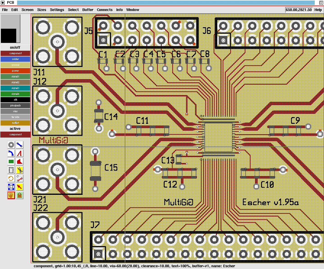
World technical: pcb version 3.0 printed circuit board layout tool
.
.
![13 Basic Rules Of PCB Layout](https://i2.wp.com/www.raypcb.com/wp-content/uploads/2018/11/a63ca0232bb6e9d.jpg)
![How Can a Printed Circuit Board Help You Test a Circuit Board Schematic?](https://i2.wp.com/www.pcbnet.com/wp-content/uploads/1/2020/06/circuit-board-schematic.jpeg)
![How to Convert PCB to Schematic Diagram? - RAYPCB](https://i2.wp.com/www.raypcb.com/wp-content/uploads/2021/03/c6c89a427ec37e0-1.png)
![Mastering the Art of PCB Design Basics | Sierra Circuits](https://i2.wp.com/www.protoexpress.com/blog/wp-content/uploads/2021/07/shutterstock_340690565-scaled.jpg)
![How to Turn a Schematic into a PCB Layout: PCB Design for a Custom](https://i2.wp.com/www.allaboutcircuits.com/uploads/articles/Hughes_Project_muRataInclinometer_Image009.jpg)
![Printed Circuit Board Design, Diagram, Assembly - Steps, Tutorial](https://i2.wp.com/www.electronicsandyou.com/blog/wp-content/uploads/2013/06/pcb-layout.jpg)
![world technical: PCB version 3.0 printed circuit board layout tool](https://4.bp.blogspot.com/-X_6cSoa9tNY/T0w4pjN8tsI/AAAAAAAADRk/xcQ53Zt3hM0/s1600/tclpcb_screen.gif)
![Make Sure to Consider These Factors When Creating a PCB Layout - Blog](https://i2.wp.com/www.pcbunlimited.com/blog/wp-content/uploads/2017/04/circuitboardprototyping.jpg)
![Printed Circuit Board Design, Diagram, Assembly - Steps, Tutorial](https://i2.wp.com/www.electronicsandyou.com/blog/wp-content/uploads/2013/06/pcb-design.jpg)
![Circuit Board Design Class - PCB Concepts and Materials - Instructables](https://i2.wp.com/content.instructables.com/ORIG/FWB/N7ZL/K6HPDIV7/FWBN7ZLK6HPDIV7.jpg)